General principles of PCB design
11 Dec 2020 -
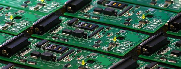
In order to achieve the best performance of electronic circuit, it is very important to arrange the components and wires. In order to design PCB with good quality and low cost, the following general principles shall be followed:
1. layout
First, the PCB size should be considered. When PCB size is too large, the printed line is long, impedance increases, noise resistance ability decreases and cost increases; if it is too small, it will not heat well and adjacent lines will be easily disturbed. After determining PCB size, the position of special components can be determined. Finally, according to the function unit of the circuit, all the components of the circuit are arranged. Single chip development PCB control board PCB circuit board scheme design LED lighting thermostat development Hongsheng photoelectric
The following principles shall be followed when determining the location of special components:
(1) The connection between high frequency components should be shortened as much as possible, and their distribution parameters and electromagnetic interference between them should be reduced. The components susceptible to interference shall not be too close to each other, and the input and output components shall be as far away as possible.
(2) There may be a high potential difference between some components or wires, so the distance between them should be increased to avoid accidental short circuit caused by discharge. Components with high voltage shall be arranged as far as possible in places not easily accessible during commissioning.
(3) Components with weight more than 15g shall be fixed with brackets and welded. Those components with large and heavy heat output should not be installed on the printed board, but on the chassis bottom of the machine, and the heat dissipation should be considered. The thermal element shall be away from the heating element.
(4) The structure requirements of the whole machine shall be considered for the layout of adjustable elements such as potentiometer, adjustable inductance coil, variable capacitor, micro switch, etc. If the adjustment is in the machine, it should be placed on the place above the printed board for easy adjustment; if the adjustment is outside the machine, its position shall be suitable for the position of the adjustment knob on the cabinet panel.
(5) The positioning holes of the printed plate and the position occupied by the fixing bracket shall be reserved.
According to the function unit of the circuit, when layout all the components of the circuit, the following principles shall be met:
(1) Arrange the position of each functional circuit unit according to the circuit flow, make the layout convenient for signal circulation and keep the signal in the same direction as possible.
(2) The core components of each function circuit are taken as the center, and the layout is carried out around it. Components shall be arranged uniformly, neatly and compactly on PCB, and lead and connection between components shall be minimized and shortened as far as possible.
(3) The distribution parameters between components should be considered for circuits working at high frequency. The general circuit shall be arranged in parallel as possible. In this way, it is not only beautiful, but also easy to assemble and weld, and easy to mass production.
(4) The components located at the edge of the circuit board shall not be less than 2mm away from the edge of the circuit board. The best shape of the circuit board is rectangle. The ratio of length to width is 3:2 to 4:3. When the size of the circuit board surface is greater than 200x150mm, the mechanical strength of the circuit board shall be considered.


